Description
Description of TFT LCD Module – 2.0″ TFT 240×320, 2.0-Inch TFT LCD
The SF-TC200L-8939A-N TFT LCD module features a 2.0-inch diagonal size display with a portrait mode resolution of QVGA 240×320, providing vibrant full-color visuals. This LCD module supports various interfaces including MCU, SPI, and RGB, with customizable options for the interface.
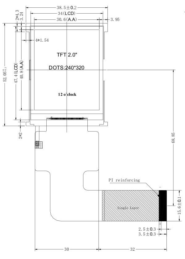
Measuring at 38.5mm in width, 52.05mm in length, and 2.95mm in thickness, the SF-TC200L-8939A-N model has a compact module dimension. The active area of the display is 30.60 x 40.80 mm.
Integrated with the ST7789V or an equivalent driver IC controller on the module, the SF-TC200L-8939A-N operates with a logic supply voltage ranging from 2.6V to 3.3V, with a typical value of 2.8V. The surface luminance is 250 cd/m2 (Nits). The operating temperature ranges from -20 to 70 degrees Celsius, while the storage temperature is between -30 to 80 degrees Celsius.
This TFT LCD model finds versatile applications in handheld devices, POS terminals, cash readers, embedded systems, home automation, GPS devices, medical equipment, industrial devices, and security equipment. It is especially suitable for applications requiring high-quality and colorful TFT displays.
Product Features
| Product: | 2.0″ Inch TFT LCD Panel Display |
|---|---|
| Resolution: | QVGA 240×320 Dots |
| Driver IC: | ST7789V IC Or Equivalent |
| Touch Screen: | Without Touch Screen (Customizable) |
| Cover Glass Dimension: | Customizable |
| Viewing Direction: | 12 O’clock |
| Outline Dim.: | 38.5(W) X 52.05(L) X 2.95(T) mm |
| Active Area: | 30.60 X 40.80 Mm |
| Interface: | MCU/SPI/RGB |
| Connection: | FPC Connector Type |
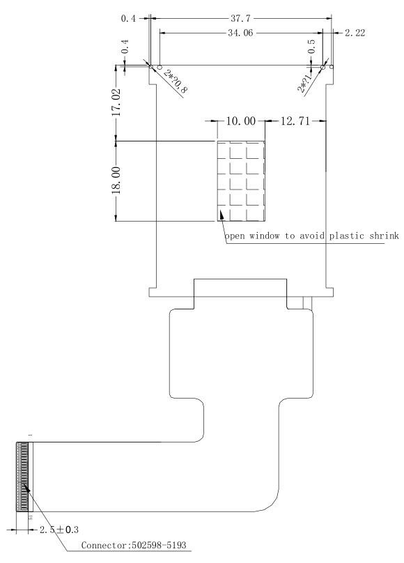
| Pin Number: | 51 Pins |
| Surface Luminance: | 250 Cd/m2(nits) |
| Operating Voltage: | 2.8 V |
| Backlight Type: | White LED |
| LED Lifetime: | 40,000 Hours |
| Compliance: | REACH & RoHS Compliant |
2″ TFT 240×320, TFT LCD 2 inch Drawing
Interface Pin Definition
| NO. | PIN NAME | Description |
| 1 | GND | Ground |
| 2-3 | VCI | Power Supply 2.8V Voltage |
| 4-5 | IOVCC | Power Supply 2.8V/1.8V Voltage |
| 6 | IM3 | Select the interface mode |
| 7 | IM2 | Select the interface mode |
| 8 | IM1 | Select the interface mode |
| 9 | IM0 | Select the interface mode |
| 10 | RESET | LCM Reset input signal |
| 11 | CS | Input pin for chip selection signal |
| 12 | RS | Register select signal |
| 13 | WR | Write strobe signal input pin |
| 14 | RD | Read strobe signal input pin |
| 15 | VSYNC | Vertical Synchronizing Signal |
| 16 | HSYNC | Horizontal Synchronizing Signal |
| 17 | ENABLE | Input Data enable control |
| 18 | DOTCLK | Clock Signal to Sample each date |
| 19 | SDA | Serial input signal |
| 20-37 | DB0-DB17 | Display Data I/O |
| 38 | TE | Tearing effect output |
| 39 | SDO | Read strobe signal input pin |
| 40 | PWM | |
| 41-42 | GND | Ground |
| 43-45 | LEDA | LED Anode |
| 46-48 | LEDK | LED Cathode |
| 49-51 | GND | Ground |
Maximum Absolute Limit
| Item | Symbol | Value | Unit |
| Power supply voltage for logic | VDD | 1.6~3.3 | V |
| Input voltage | Vin | VDD+0.3 | V |
| Operating temperature | Topr | -20 to 70 | °C |
| Storage temperature | Tstg | -30 to 80 | °C |
DC Characteristics (VDD=2.8V,Ta=25°C)
| Item | Symbol | Min | Type | Max | Unit | Test condition |
| Operating voltage | VDD | * | 2.8 | 3.3 | V | – |
| Supply current | IDD | – | – | 20 | mA | VDD=2.8V,Ta=25°C |
| Input voltage | VIH | 0.8VDD | – | VDD | V | – |
| VIL | 0 | – | 0.2VDD | V | ||
| Input leakage current | IIL | -1.0 | – | 1.0 | mA | VIN=VDD or VSS |
Backlight Electrical-optical Characteristics
| Item | Symbol | MIN | TYP | MAX | UNIT | Test Condition |
| Supply Voltage | Vf | – | 9.6 | – | V | If=20 mA |
| Supply Current | If | – | 20 | – | mA | – |
| Reverse Voltage | Vr | – | – | 5 | V | – |
| Power dissipation | Pd | – | 192 | – | mW | – |
| Luminous Intensity | – | – | 250 | – | Cd/m2 | If=20mA |
| Uniformity for LCM | – | 80 | – | – | % | If=20 mA |
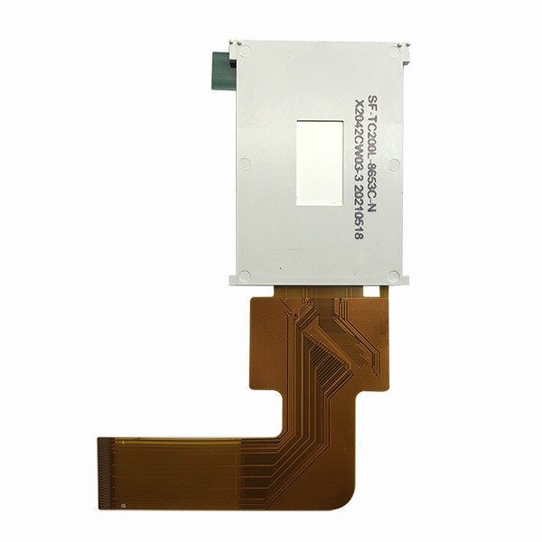
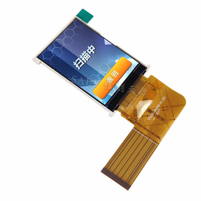
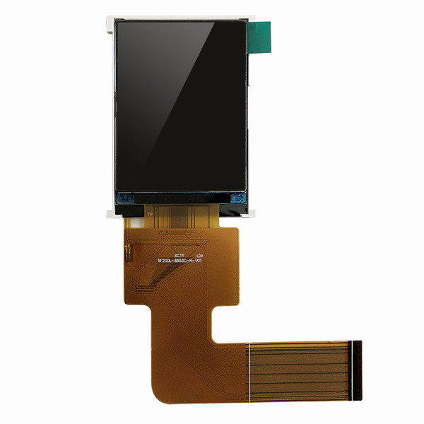
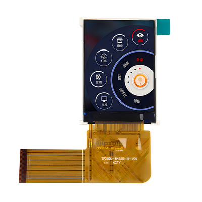
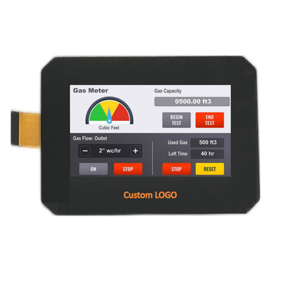
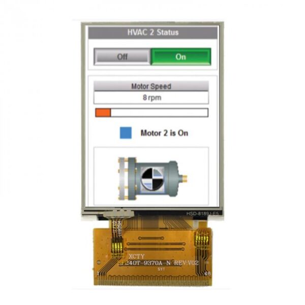
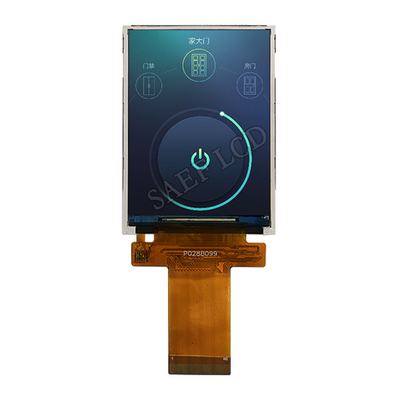
2″ TFT 240×320, TFT LCD 2 inch Product Image



Reviews
There are no reviews yet.