Description
Dive into the realm of display technology with our TFT LCD Screen, boasting a captivating 2.8-inch size and a touch-enabled interface, offering a mesmerizing resolution of 240×320 pixels, all powered by the cutting-edge ILI9341 IC and a versatile RGB/MCU interface.
Here’s a glimpse of its key specifications:
- Enthralling LCD Size: Embrace the immersive 2.8” TFT dimension.
- Resolution Wonder: Delight in the crisp 240×320 display clarity.
- Viewing Perspective: Revel in the optimal 12 O’clock viewing angle.
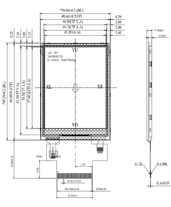
- Sleek Outline: Admire the sleek dimensions measuring 50.069.23.5.
- Driving Force: Empowered by the efficient ILI9341V Driver IC.
- Interface Harmony: Seamlessly connect with the RGB/MPU 18Bit interface.
- Touch Sensation: Experience intuitive control with the Resistive Touch Panel.
- Temperature Resilience: Endure extremes with top temperatures from -20°C to +70°C and storage temperatures from -30°C to +80°C.
Product Features
| Product: | 2.8″ Inch TFT LCD MODULE |
|---|---|
| Touch Screen: | With Resistive Touch Screen |
| Resolution: | 240×320 |
| Viewing Direction: | 12 O’clock |
| Interface: | RGB&MCU |
| Pin Number: | 50 Pins |
| Connection: | FPC Type Connection |
| Surface Luminance: | 280-350 Cd/m2 |
| Operating Temp.: | -20℃ To +70℃ |
| Compliance: | REACH & RoHS Compliant |
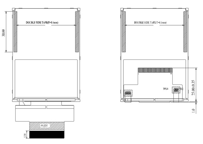
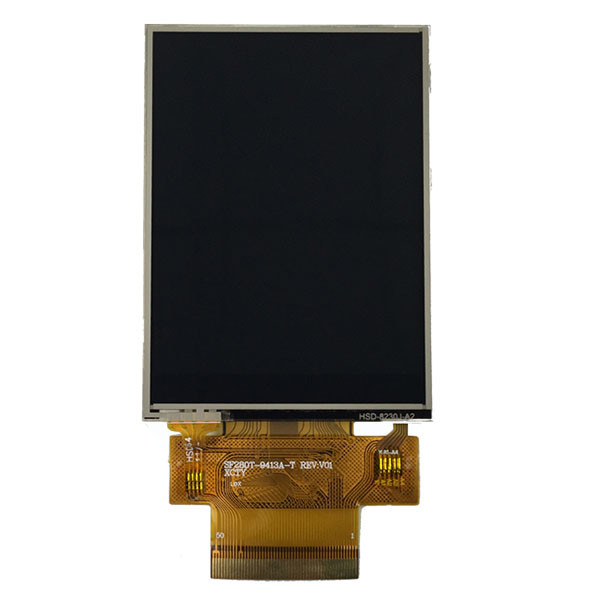
2.8″ Inch Touch LCD Display Drawing
Interface Pin Definition
| NO. | PIN NAME | I/O | Description |
| 1 | LED-K | I | LED Cathode |
| 2 | LED-A1 | I | LED Anode |
| 3 | LED-A2 | I | LED Anode |
| 4 | LED-A3 | I | LED Anode |
| 5 | LED-A4 | I | LED Anode |
| 6 | IM0 | I | System interface select. Note.1 |
| 7 | IM1 | ||
| 8 | IM2 | ||
| 9 | IM3 | ||
| 10 | RESET | I | Reset pin |
| 11 | VSYNC | I | Vertical synchronizing signal in RGB interface |
| 12 | HSYNC | I | Horizontal synchronizing signal in RGB interface |
| 13 | DOTCLK | I | Dot clock signal for RGB interface operation |
| 14 | DE | I | Data enable signal for RGB interface operation |
| 15-32 | DB0-DB17 | I/O | 18bit- Parallel data |
| 33 | SDO | I/O | Serial Output signal |
| 34 | SDI | I/O | The Data is outputted on the falling edge of the SCL signal |
| 35 | RD | I | Read strobe signal input pin |
| 36 | WR | I | Write strobe signal input pin |
| 37 | D/CX(SCL) | I | This pin is used serial interface clock in 3-wrie 9-bit/
4-wrie 8-bit serial data interface |
| 38 | CSX | I | Chip select signal |
| 39 | TE | O | Tearing effect output pin to synchronize MPU to frame
writing, activated by S/W command. |
| 40 | IOVCC | I | Power Supply1.8V/ 2.8V Voltage |
| 41 | IOVCC | I | Power Supply1.8V/ 2.8V Voltage |
| 42 | VCC | I | Power Supply 2.8V Voltage |
| 43 | GND | – | Ground |
| 44 | XR | I | Touch Panel input signal |
| 45 | YD | I | Touch Panel input signal |
| 46 | XL | I | Touch Panel input signal |
| 47 | YU | I | Touch Panel input signal |
| 48 | GND | – | Ground |
| 49 | GND | – | Ground |
| 50 | GND | – | Ground |
Maximum Absolute Limit
| Item | Symbol | Value | Unit |
| Power supply voltage for logic | VDD | 2.6~3.3 | V |
| Input voltage | Vin | VDD+0.3 | V |
| Operating temperature | Topr | -20 to 70 | °C |
| Storage temperature | Tstg | -30 to 80 | °C |
DC Characteristics (VDD=2.8V,Ta=25°C)
| Item | Symbol | Min | Type | Max | Unit | Test condition |
| Operating voltage | VDD | 2.6 | 2.8 | 3.3 | V | – |
| Supply current | IDD | – | – | 5 | mA | VDD=2.8V,Ta=25°C |
| Input voltage | VIH | 0.8VDD | – | VDD | V | – |
| VIL | 0 | – | 0.2VDD | V | ||
| Input leakage current | IIL | -1.0 | – | 1.0 | mA | VIN=VDD or VSS |
Backlight Electrical-optical Characteristics
| Item | Symbol | MIN | TYP | MAX | UNIT | Test
Condition |
Note |
| Supply Voltage | Vf | 3.0 | 3.2 | 3.4 | V | If=80 mA | – |
| Supply Current | If | – | 80 | – | mA | – | – |
| Reverse Voltage | Vr | – | – | 5 | V | – | |
| Power dissipation | Pd | – | 256 | – | mW | – | |
| Luminous Intensity for LCM |
– |
– | 280 | – | Cd/m2 | If=80mA | – |
| Uniformity for LCM | – | 80 | – | – | % | If=80mA | – |
| Backlight Color | White | ||||||
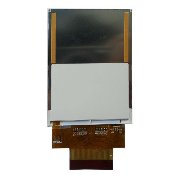
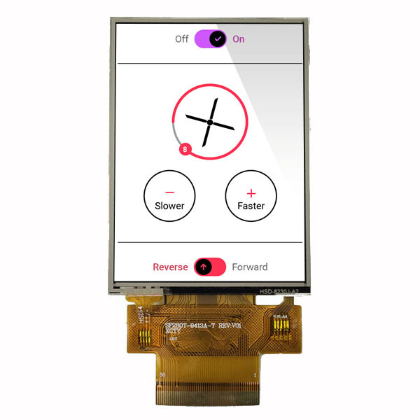
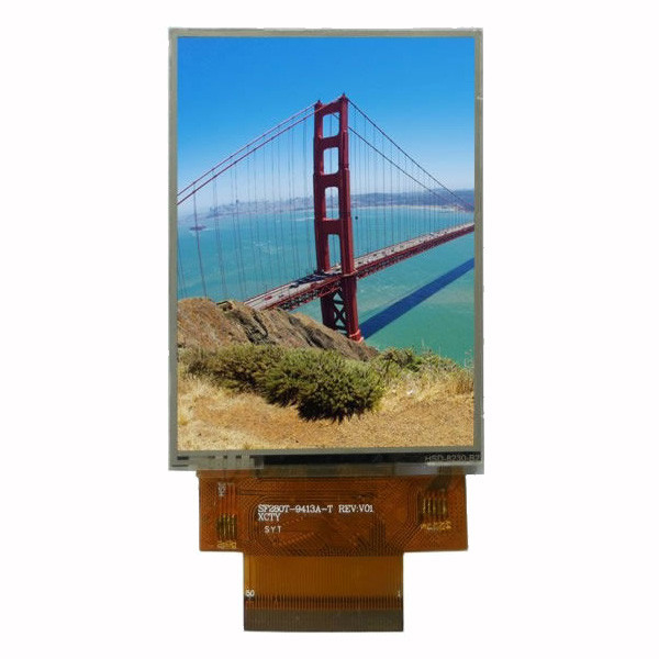
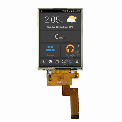
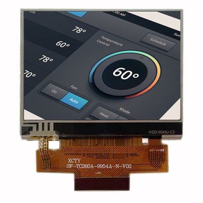
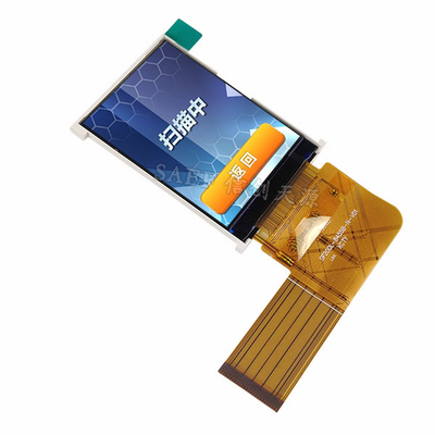
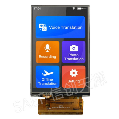
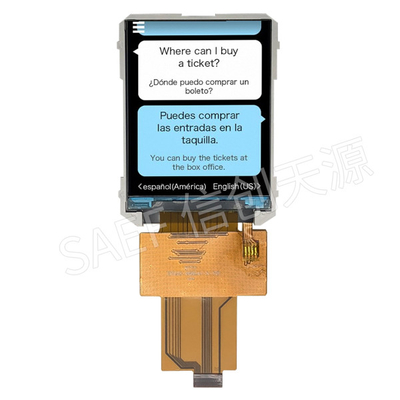
2.8″ Inch Touch LCD Display Product Image




Reviews
There are no reviews yet.