Description
12.3″ Bar Type TFT LCD for Automotive Use (SFHDMI1230H-1920720A-N)
Product Introduction
The SFHDMI1230H-1920720A-N is a 12.3-inch color active matrix TFT LCD module designed for automotive applications. It features:
- HD resolution (1920 x 720 pixels)
- 16.2M color display (6-bit + 2FRC)
- 45% color gamut
- LVDS interface
- Integrated LED backlight driver
Key Features
- Stretched “Bar Type” Design: Ideal for automotive dashboards and other applications requiring a wide format.
- LVDS Interface: Ensures compatibility with common automotive systems.
- High Brightness: 850cd/m2 for excellent visibility under various lighting conditions.
- Wide Operating Temperature Range: -30°C to +85°C for reliability in extreme environments.
- Customization: Available with a capacitive touch screen for enhanced user interaction.
Let me know if you’d like further revisions or have any specific area, you’d like a different approach to!
| Keywords: | 12.3″ Inch Bar Type TFT |
| Resolution: | 1920×720 Dots |
| Surface Luminance: | 850 Cd/m2 (nits) |
| Touch Interface: | IIC(I2C) |
| Interface: | HDMI |
| Support: | Raspberry Pi, Windows, Jetson Nano |
| Touch Screen: | 10-point Capacitive Touch Screen |
| Cover Glass Dimension: | Customizable |
| Viewing Direction: | IPS, All Viewing Angles |
| LED Lifetime: | 40,000 Hours |
| Operating Temp.: | –30℃ To +85℃ |
| Storage Temp.: | –30℃ To +85℃ |
| Certification: | ISO9001:2015 / ISO14000:2015 |
| Compliance: | REACH & RoHS Compliant & Halogen Free |
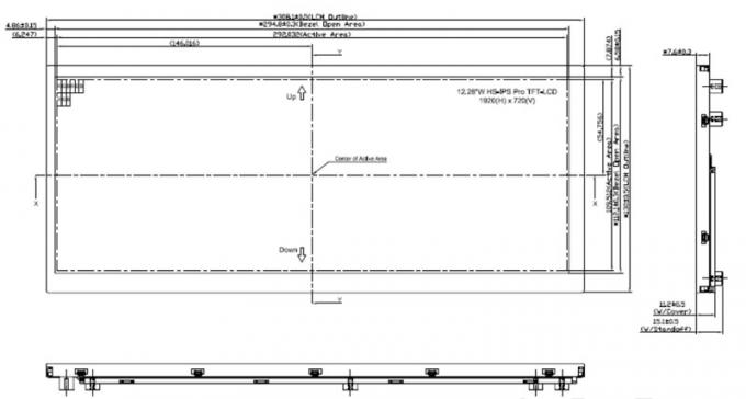
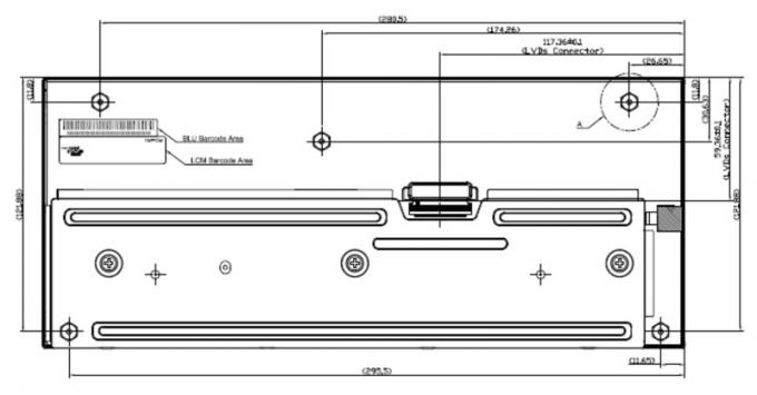
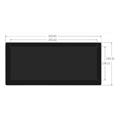
12.3″ Inch Bar Type TFT LCD 1920×720 Dots LVDS Auto Grade Screen Product Drawing
Interface Pin Definition
| Pin no. | Symbol | Function |
|---|---|---|
| 1 | GND | Ground |
| 2 | NC | No connector |
| 3 | VCC | Digital Power |
| 4 | VCC | Digital Power |
| 5 | GND | Panel Power |
| 6 | GND | Panel Power |
| 7 | NC | No connector |
| 8 | NC | No connector |
| 9 | GND | Ground |
| 10 | ORXIN0- | Odd pixel negative LVDS differential clock input |
| 11 | ORXIN0+ | Odd pixel positive LVDS differential clock input |
| 12 | ORXIN1- | Odd pixel negative LVDS differential clock input |
| 13 | ORXIN1+ | Odd pixel positive LVDS differential clock input |
| 14 | ORXIN2- | Odd pixel negative LVDS differential clock input |
| 15 | ORXIN2+ | Odd pixel positive LVDS differential clock input |
| 16 | ORXCLKIN- | Odd pixel negative LVDS differential clock input |
| 17 | ORXCLKIN+ | Odd pixel positive LVDS differential clock input |
| 18 | ORXIN3- | Odd pixel negative LVDS differential clock input |
| 19 | ORXIN3+ | Odd pixel positive LVDS differential clock input |
| 20 | ERXIN0- | Even pixel negative LVDS differential clock input |
| 21 | ERXIN0+ | Even pixel positive LVDS differential clock input |
| 22 | ERXIN1- | Even pixel negative LVDS differential clock input |
| 23 | ERXIN1+ | Even pixel positive LVDS differential clock input |
| 24 | ERXIN2- | Even pixel negative LVDS differential clock input |
| 25 | ERXIN2+ | Even pixel positive LVDS differential clock input |
| 26 | ERXCLKIN- | Even pixel negative LVDS differential clock input |
| 27 | ERXCLKIN+ | Even pixel positive LVDS differential clock input |
| 28 | ERXIN3- | Even pixel negative LVDS differential clock input |
| 29 | ERXIN3+ | Even pixel positive LVDS differential clock input |
| 30 | GND | Ground |
| 31 | NC | No connector |
| 32 | RESETB | Global reset pin, active low. |
| 33 | STBYB | Standby mode, active low. |
| 34 | CA3 | Output signal to indicate self-protection mode, when DE, HS, VS, DCLK, any of these signals is missing, it will become High. If using this pin, CA3 need to pulled low by a resistor else, let it float. |
| 35 | SCL | Serial interface clock input. (User floating) |
| 36 | SDA | Serial interface data input/output. (User floating) |
| 37 | CSB | Serial interface chip enable. (User floating) |
| 38 | GND | Power Ground |
| 39 | GND | Power Ground |
| 40 | NC | No connector |
| 41 | LEDA | LED power (Anode) |
| 42 | LEDA | LED power (Anode) |
| 43 | LEDA | LED power (Anode) |
| 44 | NC | No connector |
| 45 | LEDK1 | Cathode 1 |
| 46 | LEDK2 | Cathode 2 |
| 47 | LEDK3 | Cathode 3 |
| 48 | LEDK4 | Cathode 4 |
| 49 | NTC_A | NTC_Anode |
| 50 | NTC_K | NTC_Cathode |
PCAP PIN Definition
| Pin | Symbol | Function |
|---|---|---|
| 1 | USB_VSS | System ground |
| 2 | USB_VDD 5V | Power supply |
| 3 | USB_D+ | Data + |
| 4 | USB_D- | Data – |
| 5 | VSS | System ground |
| 6 | SDA | I2C data input and output |
| 7 | SCL | I2C clock input |
| 8 | RST | External Reset, Low is active. |
| 9 | INT | External interrupts to the host |
| 10 | VDDT 3.3 | Power supply |
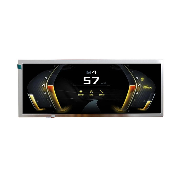
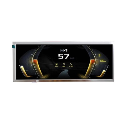
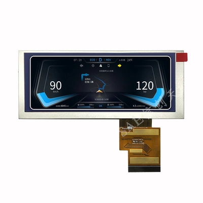
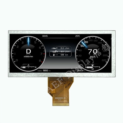
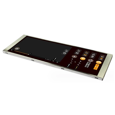
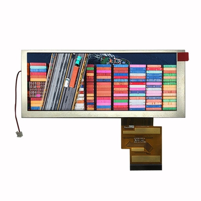
12.3″ Inch Bar Type TFT LCD 1920×720 Dots LVDS Automobile Grade Screen Product Image (without Capacitive Touch)
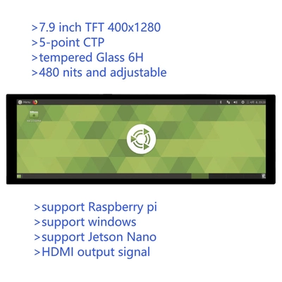
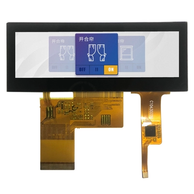
(with Capacitive Touch)



Reviews
There are no reviews yet.