Description
Unveiling the Innovation: 0.5 Inch OLED Display Module with 88×48 Resolution
Step into the future with the SFOS050XZ-7112AN OLED Display Module, boasting an impressive 88×48 resolution in a sleek 0.5-inch diagonal size. This COG graphic display isn’t just a marvel; it’s an industrial-grade powerhouse that combines cutting-edge features with a competitive price point. Embedded with the advanced CH1115 IC and supporting the versatile I2C interface, this module sets a new standard in display technology.
Powering Possibilities: Key Specifications
- Logic Supply Voltage: 2.8V
- Display Supply Voltage: 9V
- Operating Current for VDD: 180μA
- Driving Duty: 1/48
The SFOS50XZ-7112AN OEL display module is not limited by the product application environment. It is the preferred solution for wearable devices, smart home applications, and other fields. This module operates seamlessly within the temperature range of -40 ℃ to+80 ℃ and has storage capacity from -40 ℃ to+85 ℃, ensuring reliability in any environment.
| Product: | 0.5 Inch OLED Display Module |
| Number Of Pixels: | 48×88 Pixels |
| Driver IC: | CH1115 Or Equivalent |
| Display Mode: | Passive Matrix |
| Display Color: | Monochrome (white) |
| Drive Duty: | 1/48 Duty |
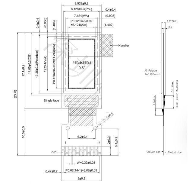
| Panel Size: | 8.928 X 17.1 X 1.227 (mm) |
| Active Area: | 6.124 X 11.244 (mm) |
| Pixel Pitch: | 0.128 X 0.128 (mm) |
| Pixel Size: | 0.108 X 0.108 (mm) |
| Viewing Direction: | All Viewing Angles |
| Interface: | I2C |
| Connection: | Soldering/Hotbar (customizable) |
| Pin Number: | 14 Pins |
| Life Time: | 50,000 Hours @60cd/m2 |
| Compliance: | REACH & RoHS Compliant |
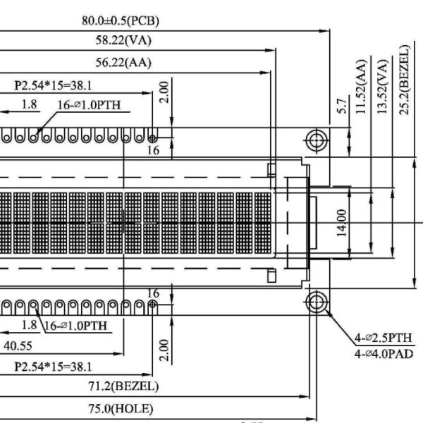
88×48 Pixels Matrix 0.5 Inch OLED Display Module Product Drawing
Pin Definition
Pin1, C2P / Pin2, C2N / Pin3, C1P / Pin4, C1N
Positive Terminal of the Flying Inverting Capacitor, Negative Terminal of the Flying Boost Capacitor. The charge-pump capacitors are required between the terminals. They must be floated when the converter is not used.
Pin5, VDD2 VBAT
Power Supply for DC/DC Converter Circuit. This is the power supply pin for the internal buffer of the DC/DC voltage converter. It must be connected to external source when the converter is used. It should be connected to VDD when the converter is not used.
Pin6, VBREF NC
Pin7, VSS
Ground of Logic Circuit. This is a ground pin. It acts as a reference for the logic pins. It must be connected to external ground.
Pin8, VDD1
Power Supply for Logic. This is a voltage supply pin. It must be connected to external source.
Pin9, RES#
Power Reset for Controller and Driver. This pin is reset signal input. When the pin is low, initialization of the chip is executed. Keep this pin pull high during normal operation.
Pin10, SCL
IIC Bus Clock Signal. The transmission if information in the I2C bus is following a clock signal. Each transmission of data bit is taken place during a single clock period of this pin.
Pin11, SDA
I2C Bus Data Signal. This pin acts as a communication channel between the transmitter and the receiver.
Pin12, IREF
Current Reference for Brightness Adjustment. This pin is a segment current reference pin. A resistor should be connected between this pin and VSS. Set the current at 12.5uA maximum.
Pin13, VCOMH
Voltage Output High Level for COM Signal. This pin is the input pin for the voltage output high level for COM signals. A capacitor should be connected between this pin and VSS.
Pin14, VCC
Power Supply for OEL Panel. This is the most positive voltage supply pin of the chip. A stabilization capacitor should be connected between this pin and VSS when the converter is used. It must be connected to external source when the converter is not used.
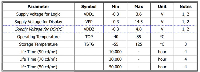
Note 1: All the above voltages are on the basis of “VSS = 0V”.
Note 2: When this module is used beyond the above absolute maximum ratings, permanent breakage of the module may occur. Also, for normal operations, it is desirable to use this module under the conditions according to Section 3. “Optics & Electrical Characteristics”. If this module is used beyond these conditions, malfunctioning of the module can occur and the reliability of the module may deteriorate.
Note 3: The defined temperature ranges do not include the polarizer. The maximum withstood temperature of the polarizer should be 80°C.
Note 4: VPP = 7.5V, Ta = 25°C, 50% Checkerboard. Software configuration follows Section 4.4 Initialization. End of lifetime is specified as 50% of initial brightness reached. The average operating lifetime at room temperature is estimated by the accelerated operation at high temperature conditions.

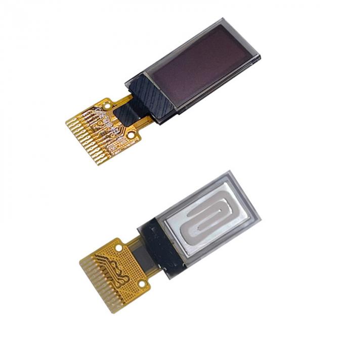
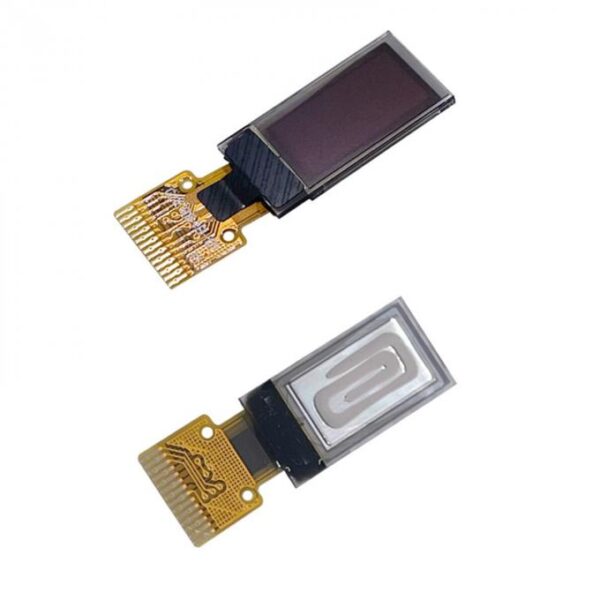
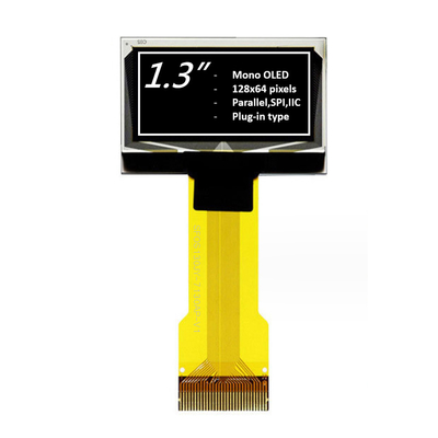
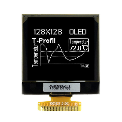
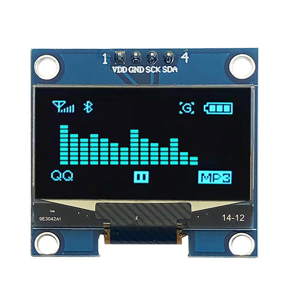
88×48 Pixels Matrix 0.5 Inch OLED Display Module Product Image


Reviews
There are no reviews yet.