Description
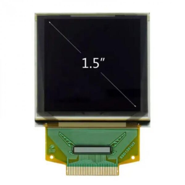
Unveiling the Cutting-Edge: 1.5 Inch AMOLED Display with 128×128 Dots and 262k Color Brilliance, Featuring the UG-2828GDEDF11 SSD1351 Controller
Product Overview
Step into the future with our state-of-the-art Organic Light-Emitting Diode (OLED) technology, delivering unparalleled brightness, crystal-clear images, and lightning-fast response times. Introducing the UG-2828GDEDF11 OLED display, a 1.5-inch marvel boasting 120 x 128 dots of vivid mono-color brilliance. This OLED module, characterized by its feather-light build, minimal power consumption, and compact design, offers a range of interface options, including default SPI, Parallel, and I2C interfaces.
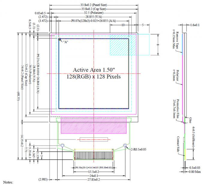
Dive into the immersive experience with an active area measuring 1.5 inches diagonally, encapsulating dimensions of 33.80 × 34.00 × 1.60 (mm). The active area itself spans 26.855 × 26.864 (mm), providing a canvas for brilliance. Equipped with the advanced IC SSD1315, this 1.5-inch OLED display showcases an impressive contrast ratio of 20,000:1. The logic supply voltage spans from 1.65V to 3.5V, with a typical value of 3V.
Application
Embrace the possibilities across various applications, from medical devices to POS systems, white goods, and home applications. This OLED display finds its niche in industrial instruments, automation, audio/visual display systems, personal care appliances, household goods, automobile displays, and dynamic information displays. Elevate your technological experience with this avant-garde display, where innovation meets excellence.
Product Features
| Product: | 1.5″ Inch Color AMOLED Display |
|---|---|
| Resolution: | 128×128 Pixels Resolution |
| Display Mode: | Passive Matrix |
| Interface: | 8-bit 68XX/80XX Parallel, 4-wire SPI, I2C |
| Display Color: | Full Color |
| Optics: | All Viewing Angles |
| Outline Dim.: | 33.80 × 34.00 × 1.60 (mm) |
| Active Area: | 26.855 × 26.864 (mm) |
| Pixel Pitch: | 0.07 × 0.21 (mm) |
| Operating Temp: | -40°C To +70°C |
| Storage Temp.: | -40°C To +85°C |
| Driver IC: | SSD1315 |
| Supply Voltage For Logic: | 1.65 – 3.5V |
| Pin Number: | 30 Pins |
| IC Package Type: | COF |
| Module Connecting Type: | ZIF |
| Duty: | 1/128 |
| Compliance: | REACH & RoHS Compliant |
1.5 Inch 128×128 Dots 262k Color SSD1351 AMOLED Display Product Drawing
Interface Pin Definition
| Pin Number | Symbol | Type |
Function |
||
| Power Supply | |||||
|
27 |
VCI |
P |
Power Supplyfor Operation
This is a voltage supply pin. It must be connected to external source & always be equal to or higher than VDD & VDDIO. |
||
|
26 |
VDD |
P |
Power Supplyfor Core Logic Circuit
This is a voltage supply pin which is regulated internally from VCI. A capacitor should be connected between this pin & VSS under all circumstances. |
||
|
4 |
VDDIO |
P |
Power Supplyfor I/OPin
This pin is a power supply pin of I/O buffer. It should be connected to VCI or external source. All I/O signal should have VIH reference to VDDIO. When I/O signal pins (BS0~BS1, D0~D7, control signals…) pull high, they should be connected to VDDIO. |
||
|
28 |
VSS |
P |
Ground of OEL System
This is a ground pin. It also acts as a reference for the logic pins, the OEL driving voltages, and the analog circuits. It must be connected to external ground. |
||
| 2 | VCC | P | Power Supplyfor OEL Panel
This is the most positive voltage supply pin It must be connected to external source. |
of the chip | |
| Driver | |||||
|
22 |
IREF |
I |
Current Referencefor Brightness Adjustment
This pin is segment current reference pin. A resistor should be connected between this pin and VSS. Set the current lower than 12.5uA. |
||
|
3 |
VCOMH |
P |
Voltage Ouut High Levelfor COM Signal
This pin is the input pin for the voltage output high level for COM signals. A tantalum capacitor should be connected between this pin and VSS. |
||
|
5 |
VSL |
P |
Voltage Ouut Low Levelfor SEG Signal
This is segment voltage reference pin. When external VSL is not used, this pin should be left open. When external VSL is used, this pin should connect with resistor and diode to ground. |
||
| External IC Control | |||||
|
24 23 |
GPIO0 GPIO1 |
I/O |
General Purpose Input/Ouut
These pins could be left open individually or have signal inputted/outputted. They are able to use as the external DC/DC converter circuit enabled/disabled control or other applications. |
||
| Interface | ||||||
|
17 18 |
BS0 BS1 |
I |
Communicating Protocol Select
These pins are MCU interface selection input. See the following table: |
|||
| BS0 | BS1 | |||||
| 3-wire SPI | 1 | 0 | ||||
| 4-wire SPI | 0 | 0 | ||||
| 68XX-parallel (8-bit) | 1 | 1 | ||||
| 80XX-parallel (8-bit) | 0 | 1 | ||||
| 21 | RES# | I | Power Reset for Controller and Driver
This pin is reset signal input. When the pin is low, initialization of the chip is executed. |
|||
|
19 |
CS# |
I |
Chp Select
This pin is the chip select input. The chip is enabled for MCU communication only when CS# is pulled low. |
|||
|
20 |
D/C# |
I |
Data/Command Control
This pin is Data/Command control pin. When the pin is pulled high, the input at D7~D0 is treated as display data. When the pin is pulled low, the input at D7~D0 will be transferred to the command register. For detail relationship to MCU interface signals, please refer to the Timing Characteristics Diagrams. When 3-wire serial mode is selected, this pin must be connected to VSS. |
|||
|
15 |
E/RD# |
I |
Read/Write Enable or Read
This pin is MCU interface input. When interfacing to a 68XX-series microprocessor, this pin will be used as the Enable (E) signal. Read/write operation is initiated when this pin is pulled high and the CS# is pulled low. When connecting to an 80XX-microprocessor, this pin receives the Read (RD#) signal. Data read operation is initiated when this pin is pulled low and CS# is pulled low. When serial mode is selected, this pin must be connected to VSS. |
|||
|
16 |
R/W# |
I |
Read/Write Select or Write
This pin is MCU interface input. When interfacing to a 68XX-series microprocessor, this pin will be used as Read/Write (R/W#) selection input. Pull this pin to “High” for read mode and pull it to “Low” for write mode. When 80XX interface mode is selected, this pin will be the Write (WR#) input. Data write operation is initiated when this pin is pulled low and the CS# is pulled low. When serial mode is selected, this pin must be connected to VSS. |
|||
|
7~14 |
D7~D0 |
I/O |
Host Data Input/Ouut Bus
These pins are 8-bit bi-directional data bus to be connected to the microprocessor’s data bus. When serial mode is selected, D1 will be the serial data input SDIN and D0 will be the serial clock input SCLK. Unused pins must be connected to VSS except for D2. |
|||
| Reserve | |||||
| 6, 25, 29 | N.C. |
– |
Reserved Pin
The N.C. pins between function compatible and flexible design. |
pins are reserved | |
|
1, 30
|
N.C. (GND) |
– |
Reserved Pin (Supporting Pin)
The supporting pins can reduce the influences from stresses on the function pins. These pins must be connected to external ground. |
||
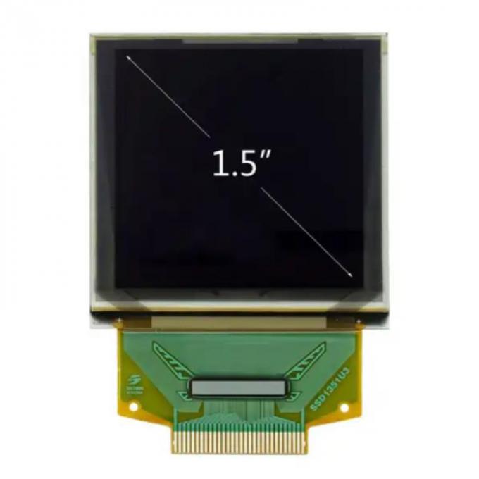
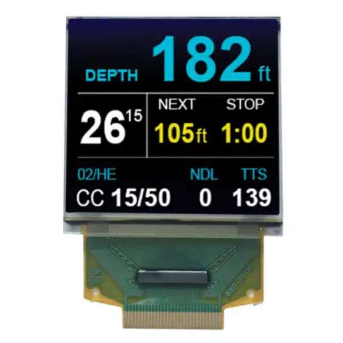
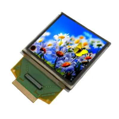
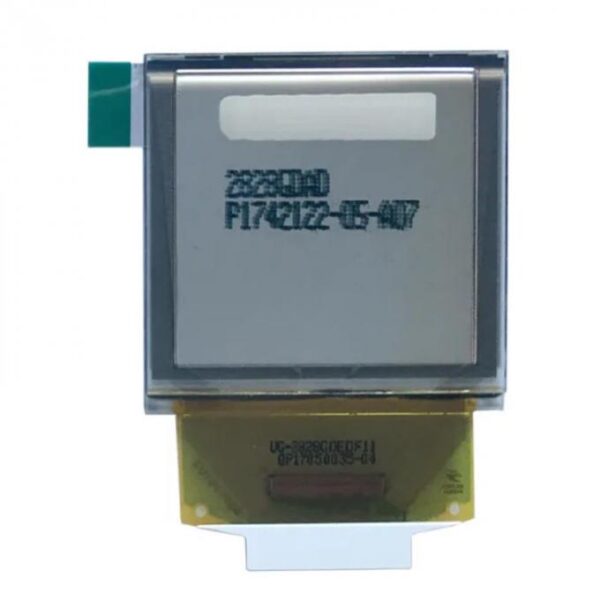
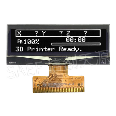
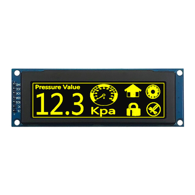
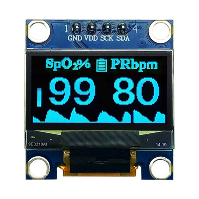
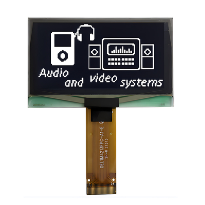
1.5 Inch 128×128 Dots 262k Color SSD1351 AMOLED Display Product Image




Reviews
There are no reviews yet.