Description
2.13 Inch Three-Color E-Paper Display: Ideal for Retail and Beyond
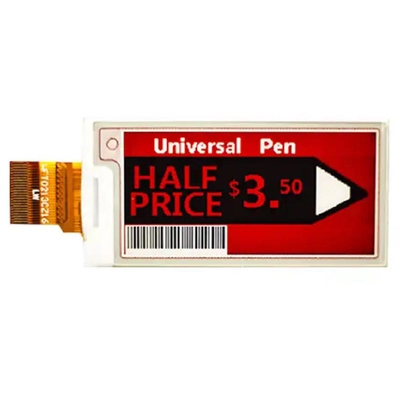
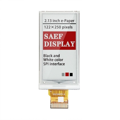
Upgrade your displays with the ShenZhen Techstar Electronics Incorporated Co., Ltd SFEPD213BWY-7018A01, a versatile 2.13-inch E-Paper display featuring three colors (white, black, and red). This high-resolution (131dpi) screen boasts:
- Energy Efficiency: Ultra-low power consumption. The display only uses power when the image changes and requires none to maintain it.
- Exceptional Readability: Super-wide viewing angle (near 180°) ensures clarity from any direction.
- Sleek Design: Extra thin and light, ideal for integration into various devices.
- Easy Connection: SPI interface for seamless compatibility.
- Environmentally Conscious: RoHS compliant.
Key Applications:
- Electronic Shelf Labels: Create dynamic, eye-catching price and product information displays.
- E-Readers: Enjoy a paper-like reading experience.
- E-Notebooks: Capture notes and sketches with a natural feel.
- Wearables: Integrate information displays into compact devices.
- And More!
Let this innovative E-Paper display transform your retail, product design, and creative projects!
| Product: | EPD 2.13″ inch | ||
|---|---|---|---|
| Resolution: | 122×250 Dots Resolution | ||
| Display Mode: | Active Matrix Electrophoretic Display(AM EPD) | ||
| Optics: | All Viewing Angles | ||
| Outline Dim.: | 29.2(H)x59.2(V)x1.0(D) Mm | ||
| Active Area: | 23.705(H)x48.55(V) Mm | ||
| Operating Temp: | 0°C To +50°C | ||
| Storage Temp: | -25°C To +60°C | ||
| Pin Number: | 24 Pins | ||
| Interface: | SPI | ||
2.13 Inch Three-Color E-Paper E-Ink Screen, 2.13” ePaper Display 250×122 Dots Drawing

Interface Pin Definition
| No. | Signal | Type | Connected to | Function |
| 1 | NC | – | – | Not connected |
| 2 | GDR | O | Power MOSFET Driver control | This pin is the N-Channel MOSFET Gate Drive Control. |
| 3 | RESE | I | Booster Control Input | This pin is the Current Sense Input for the Control Loop. |
| 4 | NC | – | – | Not connected |
| 5 | VSHR | C | Capacitor | This pin is the Positive Gate driving voltage and the Power Supply pin for VSH2. A stabilizing capacitor should be connected between VSH2 and GND. |
| 6 | TSCL(NC) | – | – | – |
| 7 | TSDA(NC) | – | – | – |
| 8 | BS | I | VSS | This pin is setting panel interface. |
| 9 | BUSY | O | Device Busy Signal | This pin is Busy state output pin. When Busy is High, the operation of the chip should not be interrupted, and Command should not be sent. |
| 10 | RES_N | I | System Reset | This pin is reset signal input.Active Low. |
| 11 | D/C | I | VDDIO or VSS | This pin is Data/Command control |
| 12 | CSB | I | VDDIO or VSS | This pin is the chip select. |
| 13 | SCL | I | Data Bus | Serial communication clock input. |
| 14 | SDA | I | Data Bus | Serial communication data
input/output. |
| 15 | VDDIO | P | Power Supply | Power for interface logic pins& I/O. It should be connected with VCI. |
| 16 | VCI | P | Power Supply | Power Supply for the chip. |
| 17 | GND | P | Ground | Ground |
| 18 | VDDD | C | Capacitor | Internal regulator output. A capacitor should be connected between VDD and GND. |
| 19 | VPP(NC) | – | – | – |
|
20 |
VSH | C | Capacitor | This pin is the Positive Source driving voltage. A stabilizing capacitor should be connected between VSH and GND. |
| 21 | VGH | C | Capacitor | A stabilizing capacitor should be connected between VGH and GND. |
|
22 |
VSL |
C |
Capacitor |
This pin is the Negative Source driving voltage and the Power Supply pin for VCOM. A stabilizing capacitor should be connected between VSL and GND. |
| 23 | VGL | C | Capacitor | A stabilizing capacitor should be connected between VGL and GND. |
|
24 |
VCOM |
C |
Capacitor |
This pin is the VCOM driving voltage. A stabilizing capacitor should be connected between VCOM and GND. |
2.13 Inch Three-Color E-Paper E-Ink Screen, 2.13” ePaper Display 250×122 Dots Image


Reviews
There are no reviews yet.