Description
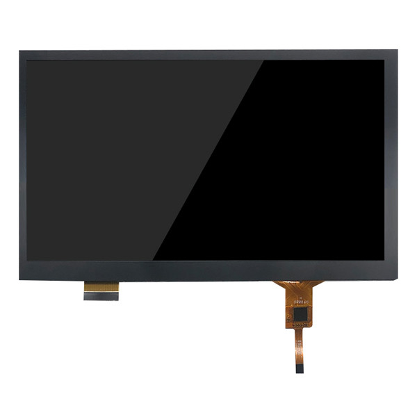
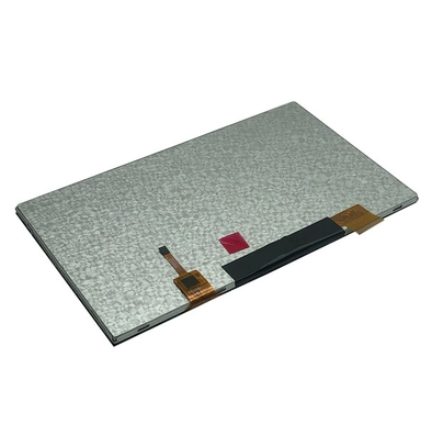
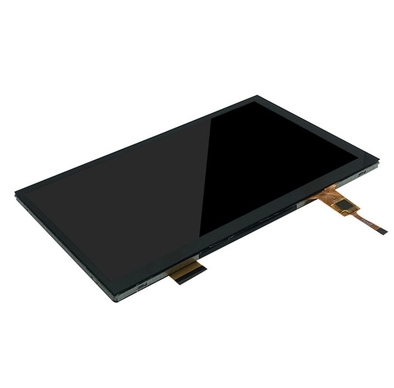
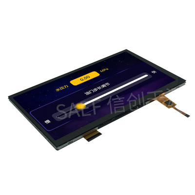
7″ inch MIPI Interface Capacitive Touch Screen TFT Display Introduction
Product Quick Insight:
- Model No. SF-TO700GLTB-8976A-CT
- Size: 7 inch
- Resolution: 1024 x 600 dots
- Interface: MIPI
- View Direction: IPS, All viewing angles
- Brightness(cd/m²): 500, (300nits, 1000nits optional)
- Touch Screen: Projected Capacitive Touch Panel (PCAP)
- Detect Point: 5 Fingers
Description:
1, ShenZhen Techstar Electronics Incorporated Co., Ltd SF-TO700GLTB-8976A-CT is a 7 inch IPS type full viewing angle TFT LCD Display with resolution of 1024×600 pixels. It is with Capacitive Touch Screen (CTP), and the cover glass is customizable.
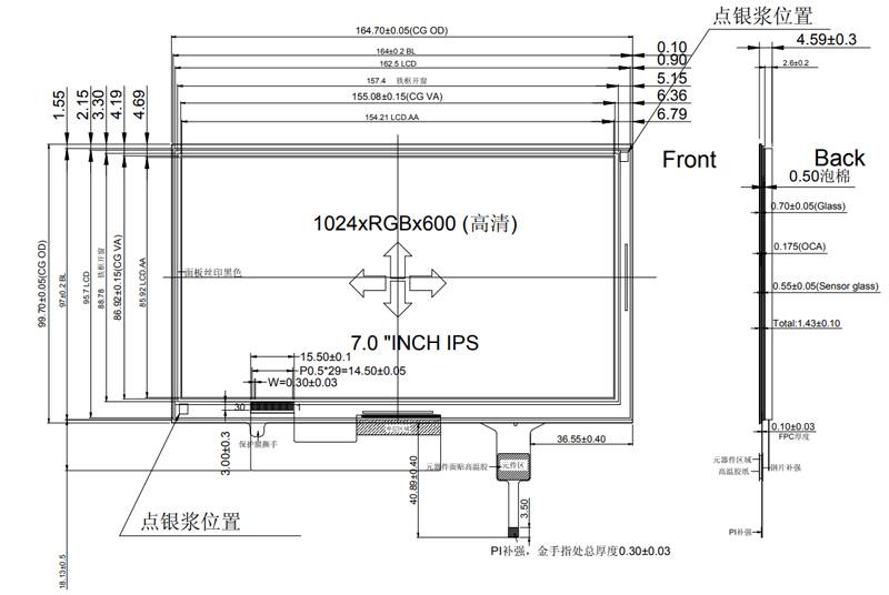
2, SF-TO700GLTB-8976A-CT TFT LCD module has outline dimension of 164.7*99*2.6 mm, and AA size of 154.21×85.92 mm.
3, SF-TO700GLTB-8976A-CT LCM interface is with MIPI interface, 30 pins. The CTP interface is I2C.
4, SF-TO700GLTB-8976A-CT touch screen is with 500cd/m2 (nits) surface brightness, it also can be designed to be 1000cd/m2 (nits). pls contact our salesperson for more details.
5, This 7” TFT LCD module is widely used in measuring equipment, medical device, home automation, access security system, supermarket price tag, and household appliances, GPS device, etc.
Features:
| Product: | 7″ Inch PCAP Touch Screen |
| TFT Interface: | MIPI |
| Surface Luminance: | 500 Cd/m2 |
| Cover Glass Dimension: | Customizable |
| Viewing Direction: | IPS All Viewing Angle (80/80/80/80) |
| Operating Temp.: | –20℃ To +70℃ |
| Resolution: | 1024×600 |
| CTP Interface: | I2C Interface |
| Touch Screen: | CTP (Capacitive Touch Screen) |
| Pins: | 30 |
| LED Lifetime: | 40,000 Hours |
| Compliance: | REACH & RoHS Compliant |
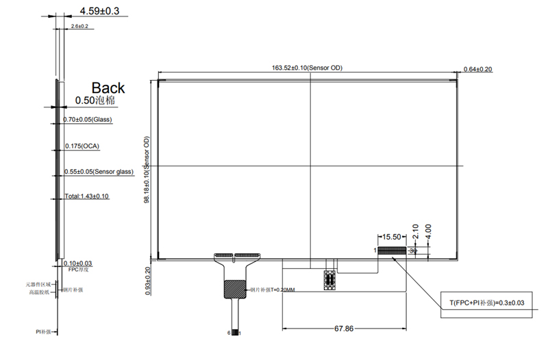
7 Inch Capacitive Touchscreen TFT LCD Module MIPI Interface Product Drawing
LCM PIN Definition
| Pin No. | Symbol | Function |
| 1 | VLED+ | LED Anode |
| 2 | VLED+ | LED Anode |
| 3 | VGH | Positive power for TFT |
| 4 | VGL | Negative power for TFT |
| 5 | UPDN | Gate up or down scan control. UPDN = ”L”, STV2 output vertical start pulse and UD pin output logical “L” to Gate driver. (default) UPDN = ”H”, STV1 output vertical start pulse and UD pin output logical “H” to Gate driver |
| 6 | SHLR | Source right or left sequence control. SHLR = ”L“, shift left: last data = S1←S2←S3……….←S1536 = first data. SHLR = ”H“, shift right: first data = S1→S2→S3……..→S1536 = last data.(default) |
| 7 | VLED- | LED Cathode |
| 8 | VLED- | LED Cathode |
| 9 | AVDD | Power for Analog Circuit |
| 10 | GND | Ground |
| 11 | D3P | MIPI data input. |
| 12 | D3N | MIPI data input. |
| 13 | GND | Ground |
| 14 | D2P | MIPI data input. |
| 15 | D2N | MIPI data input. |
| 16 | GND | Ground |
| 17 | CLKP | MIPI clock input |
| 18 | CLKN | MIPI clock input |
| 19 | GND | Ground |
| 20 | D1P | MIPI data input. |
| 21 | D1N | MIPI data input. |
| 22 | GND | Ground |
| 23 | D0P | MIPI data input. |
| 24 | D0N | MIPI data input. |
| 25 | GND | Ground |
| 26 | STBYB | Standby mode. STBYB = ”H“, normal operation(default) STBYB = ”L”, timing controller, source driver will turn off, all output are GND. |
| 27 | RESET | Global reset pin. Active Low to enter Reset State. Normally pull high. Connecting with an RC reset circuit for stability. |
| 28 | VDD(1.8V) | Digital circuit |
| 29 | VDD(1.8V) | Digital circuit |
| 30 | VCOMIN | Common voltage |
DC Characteristics (VDD=2.8V,Ta=25°C)
| Item | Symbol | Min | Type | Max | Unit | Test condition |
| Operating voltage | VDD | 2.6 | 2.8 | 3.3 | V | – |
| Supply current | IDD | – | – | 5 | mA | VDD=2.8V,Ta=25°C |
| Input voltage | VIH | 0.8VDD | – | VDD | V | – |
| VIL | 0 | – | 0.2VDD | V | ||
| Input leakage current | IIL | -1.0 | – | 1.0 | mA | VIN=VDD or VSS |
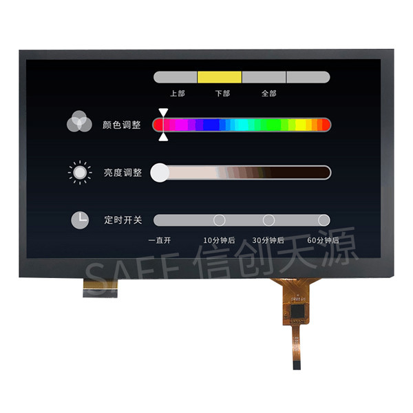
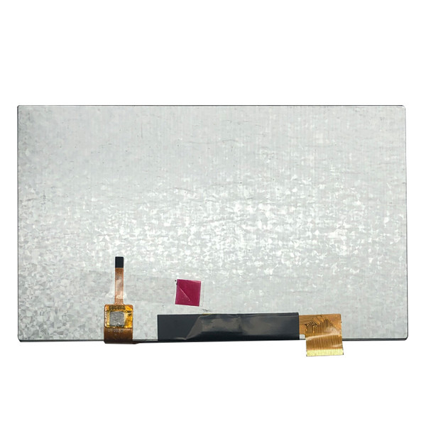
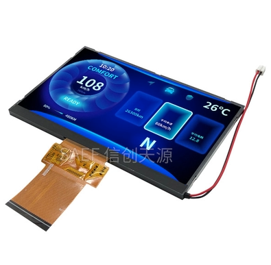
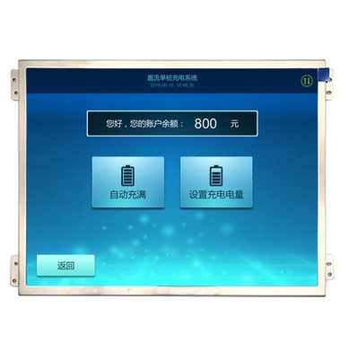
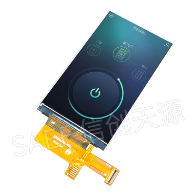
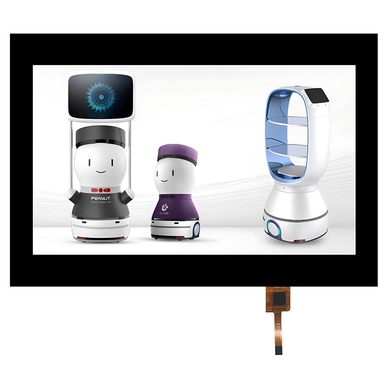
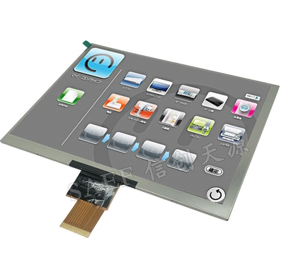
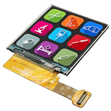
7 Inch Capacitive Touchscreen TFT LCD Module MIPI Interface Product Image


Reviews
There are no reviews yet.