Description
2 Inch IPS TFT Screen QVGA 240×320 SPI MCU RGB Interface LCD Display
Description of 2-inch IPS TFT Display, TFT LCD 2″
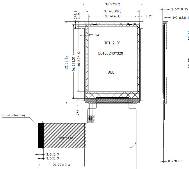
The SF-TC200H-8844A-N model presents a 2-inch diagonal full-color 240×320 QVGA TFT LCD screen module. Within its compact frame, measuring 38.5×52.05×2.6 mm, and an active area size of 30.6×40.8 mm, this TFT LCD module integrates the ST7789V IC, supporting SPI, RGB, and MCU Interface.
Configured in portrait mode, this 2” TFT LCD module offers a peak brightness of up to 300 cd/m2 nits (typical value) and functions reliably within a temperature range of -20℃ to +70℃, with storage temperatures spanning from -30℃ to +80℃.
The SF-TC200H-8844A-N model, a TFT screen 2-inch variant, is devoid of a Touch Screen TFT LCD module; however, customization options are available upon customer request to incorporate either resistive touch or capacitive touch screen functionalities. Notably, this LCD module features an anti-glare surface panel, providing optimal viewing angles and an IPS display suitable for all orientations.
Product Information
| Product: | 2 Inch TFT LCD Display |
|---|---|
| Touch Screen: | Without Touch Panel |
| Resolution: | 240×320 |
| Cover Glass Dimension: | Customizable |
| Viewing Direction: | All Viewing Direction ( IPS) |
| Interface: | SPI, MCU, RGB |
| Pin Number: | 51 Pins |
| Connection: | Plugging |
| Surface Luminance: | 300 Cd/m2 (nits) |
| LED Lifetime: | 40,000 Hours |
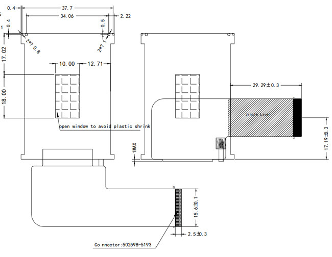
IPS 2 inch TFT Display 240×320 Pixels, TFT LCD 2″ Product Drawing
Interface Pin Definition
| NO. | PIN NAME | I/O | Description |
| 1-2 | GND | I | Ground |
| 3-4 | VCI | I | Power Supply 2.8V Voltage |
| 5-6 | IOVCC | I | Power Supply 2.8V/1.8V Voltage |
| 7 | GND | I | Ground |
| 8-11 | IM3-IM0 | I | The MCU interface mode select |
| 12 | RESET | I | LCM Reset input signal |
| 13 | CS | I | Input pin for chip selection signal |
| 14 | RS | I | Display data/command selection pin in parallel interface. |
| 15 | WR | I | Write enable in MCU parallel interface. |
| 16 | RD | I | -Read enable in 8080 MCU parallel interface |
| 17 | VSINC | I | Vertical Synchronizing Signal |
| 18 | HSYNC | I | Horizontal Synchronizing Signal |
| 19 | ENABLE | I | Input Data enable control |
| 20 | DOTCLK | I | Clock Signal to Sample each date |
| 21 | SDA | I | SPI Interface Input Pin |
| 22-39 | DB0-DB17 | I/O | Display Data I/O |
| 40 | TE | I | Tearing effect output pin |
| 41 | SDO | I | Read strobe signal input pin |
| 42 | LED_PWM | I | -Output pad for PWM output signal to driving LED. |
| 43 | LED_ON | I | Output pad for enabling LED |
| 44-45 | GND | I | Ground |
| 46-47 | LEDK | I | LED Cathode |
| 48-49 | LEDA | I | LED Anode |
| 50-51 | GND | I | Ground |
Maximum Absolute Limit
| Item | Symbol | Value | Unit |
| Power supply voltage for logic | VDD | 1.6~3.3 | V |
| Input voltage | Vin | VDD+0.3 | V |
| Operating temperature | Topr | -20 to 70 | °C |
| Storage temperature | Tstg | -30 to 80 | °C |
DC Characteristics (VDD=2.8V,Ta=25°C)
| Item | Symbol | Min | Type | Max | Unit | Test Condition |
| Operating voltage | VDD | * | 2.8 | 3.3 | V | – |
| Supply current | IDD | – | – | 20 | mA | VDD=2.8V,Ta=25°C |
| Input voltage | VIH | 0.8VDD | – | VDD | V | – |
| VIL | 0 | – | 0.2VDD | V | ||
| Input leakage current | IIL | -1.0 | – | 1.0 | mA | VIN=VDD or VSS |
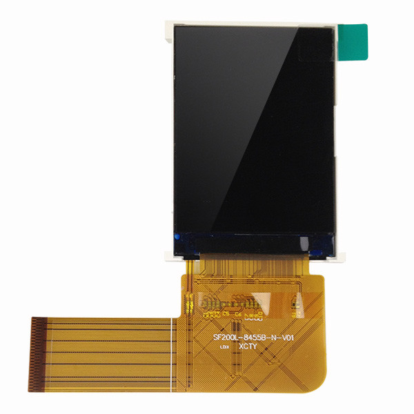
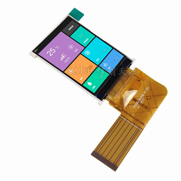
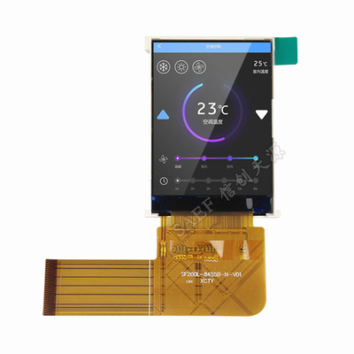
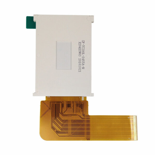
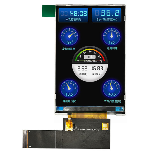
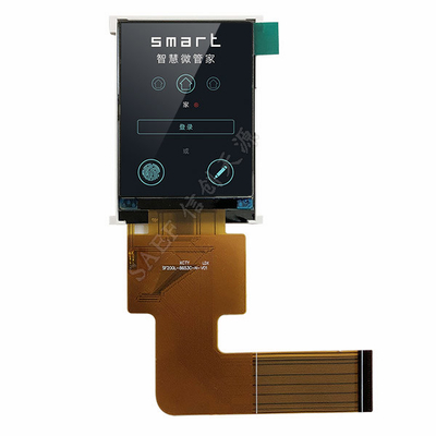
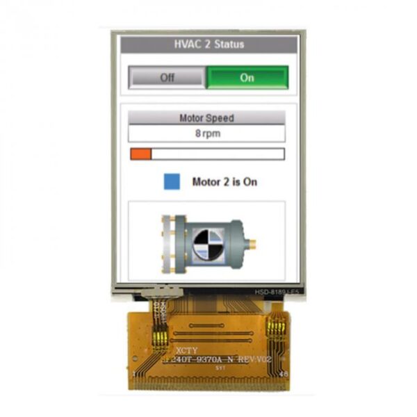
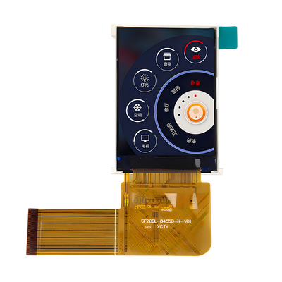
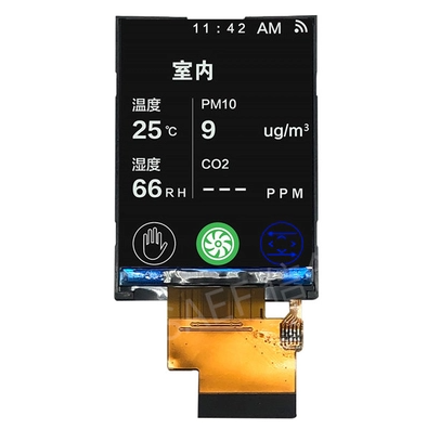
IPS 2 inch TFT Display 240×320 Pixels, TFT LCD 2″ Product Image



Reviews
There are no reviews yet.