Description
Introducing the SFHDMI1230H-1920720A-CT: A Cutting-Edge 12.3″ TFT LCD Display
Explore the Essentials:
- LCD Size: 12.3 inches TFT
- Resolution: 1920×720 pixels
- Viewing Angle: all viewing angles
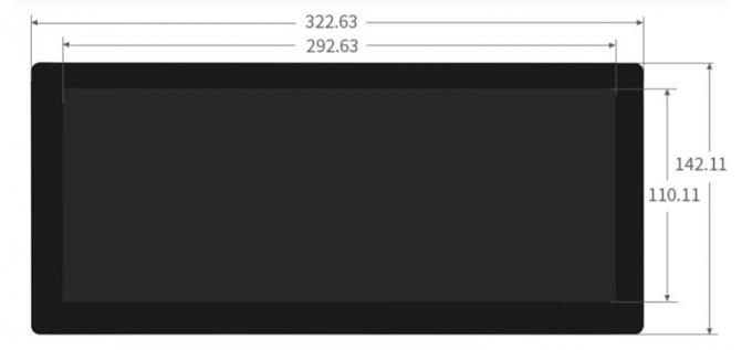
- Dimensions: 322.63×142.11×10.48 mm (LxWxD)
- LCD Driver IC: Powered by ILI2511
- Interface: LVDS
- Temperature Range: Operating between -30°C to +85°C; Storage from -30°C to +85°C
- Touch Panel: Customize with or without touch functionality for tailored experiences.
Description
SFHDMI1230H-1920720A-CT is a 12.3 inch High Brightness 1920 x 720 IPS TFT-LCD module with projected capacitive touch panel (PCAP). This module supports 2-lane LVDS(Low-Voltage-Differential-Signaling) interface which becomes more popular for larger size of TFT LCD display. The LVDS interface is a great solution because of its high speed of data transmission while using low voltage and improved noise performance. The LVDS interface has several benefits for TFT displays. It is much less susceptible to EMI and crosstalk issues, and peripherals in need of high bandwidth, like high-definition graphics and fast frame rates, allowing the transmitting device to be located farther from the display. As to the capacitive touch panel of this module is built-in with ILI2511 IC which can communicate via USB or I2C interface, supports 10 detect points.
Product information:
| Keywords: | 12.3″ Inch Bar Type TFT |
| Resolution: | 1920×720 Dots |
| Surface Luminance: | 850 Cd/m2 (nits) |
| Touch Interface: | IIC(I2C) |
| Interface: | HDMI |
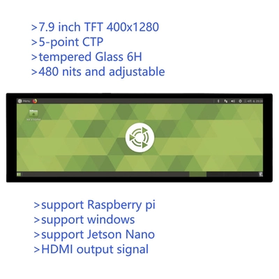
| Support: | Raspberry Pi, Windows, Jetson Nano |
| Touch Screen: | 10-point Capacitive Touch Screen |
| Cover Glass Dimension: | Optional For Customization |
| Viewing Direction: | All Viewing Angles |
| LED Lifetime: | 40,000 Hours |
| Operating Temp.: | –30℃ To +85℃ |
| Storage Temp.: | –30℃ To +85℃ |
| Certification: | ISO9001:2015 / ISO14000:2015 |
| Compliance: | REACH & RoHS Compliant & Halogen Free |
| Model Number: | SFHDMI1230H-1920720A-CT |
12.3 inch LVDS TFT High Brightness Display with PCAP Product Drawing
Interface Pin Definition
| Pin no. | Symbol | Function |
|---|---|---|
| 1 | GND | Ground |
| 2 | NC | No connector |
| 3 | VCC | Digital Power |
| 4 | VCC | Digital Power |
| 5 | GND | Panel Power |
| 6 | GND | Panel Power |
| 7 | NC | No connector |
| 8 | NC | No connector |
| 9 | GND | Ground |
| 10 | ORXIN0- | Odd pixel negative LVDS differential clock input |
| 11 | ORXIN0+ | Odd pixel positive LVDS differential clock input |
| 12 | ORXIN1- | Odd pixel negative LVDS differential clock input |
| 13 | ORXIN1+ | Odd pixel positive LVDS differential clock input |
| 14 | ORXIN2- | Odd pixel negative LVDS differential clock input |
| 15 | ORXIN2+ | Odd pixel positive LVDS differential clock input |
| 16 | ORXCLKIN- | Odd pixel negative LVDS differential clock input |
| 17 | ORXCLKIN+ | Odd pixel positive LVDS differential clock input |
| 18 | ORXIN3- | Odd pixel negative LVDS differential clock input |
| 19 | ORXIN3+ | Odd pixel positive LVDS differential clock input |
| 20 | ERXIN0- | Even pixel negative LVDS differential clock input |
| 21 | ERXIN0+ | Even pixel positive LVDS differential clock input |
| 22 | ERXIN1- | Even pixel negative LVDS differential clock input |
| 23 | ERXIN1+ | Even pixel positive LVDS differential clock input |
| 24 | ERXIN2- | Even pixel negative LVDS differential clock input |
| 25 | ERXIN2+ | Even pixel positive LVDS differential clock input |
| 26 | ERXCLKIN- | Even pixel negative LVDS differential clock input |
| 27 | ERXCLKIN+ | Even pixel positive LVDS differential clock input |
| 28 | ERXIN3- | Even pixel negative LVDS differential clock input |
| 29 | ERXIN3+ | Even pixel positive LVDS differential clock input |
| 30 | GND | Ground |
| 31 | NC | No connector |
| 32 | RESETB | Global reset pin, active low. |
| 33 | STBYB | Standby mode, active low. |
| 34 | CA3 | Output signal to indicate self protection mode, when DE,HS,VS,DCLK, any of these signals is missing, it will become High. If using this pin, CA3 need to pulled low by an resistor,else , let it floating. |
| 35 | SCL | Serial interface clock input. (User folating) |
| 36 | SDA | Serial interface data input/output.(User folating) |
| 37 | CSB | Serial interface chip enable.(User folating) |
| 38 | GND | Power Ground |
| 39 | GND | Power Ground |
| 40 | NC | No connector |
| 41 | LEDA | LED power (Anode) |
| 42 | LEDA | LED power (Anode) |
| 43 | LEDA | LED power (Anode) |
| 44 | NC | No connector |
| 45 | LEDK1 | Cathode 1 |
| 46 | LEDK2 | Cathode 2 |
| 47 | LEDK3 | Cathode 3 |
| 48 | LEDK4 | Cathode 4 |
| 49 | NTC_A | NTC_Anode |
| 50 | NTC_K | NTC_Cathode |
PCAP PIN Definition
| Pin | Symbol | Function |
|---|---|---|
| 1 | USB_VSS | System ground |
| 2 | USB_VDD 5V | Power supply |
| 3 | USB_D+ | Data + |
| 4 | USB_D- | Data – |
| 5 | VSS | System ground |
| 6 | SDA | I2C data input and output |
| 7 | SCL | I2C clock input |
| 8 | RST | External Reset, Low is active |
| 9 | INT | External interrupt to the host |
| 10 | VDDT 3.3 | Power supply |
Electrical Characteristics
| Item | Symbol | Min. | Typ. | Max. | Unit |
|---|---|---|---|---|---|
| Supply Voltage | VCC | 3 | 3.3 | 3.6 | V |
| Input signal voltage | ViH | VCC *0.7 | – | VCC | V |
| ViL | 0 | – | VCC *0.3 | V | |
| Current of power supply | ICC | – | – | 500 | mA |
| Inrush current | IRUSH | – | – | 2.0 | A |
| Supply CTP(USB) | USB_VDD 5V | 4.75 | 5.0 | 5.25 | V |
| I USB_VDD | – | 90 | 135 | mA | |
| Supply CTP(I2C) | VDDT 3.3 | 3.15 | 3.3 | 3.45 | V |
| IVDDT | – | 90 | 135 | mA |
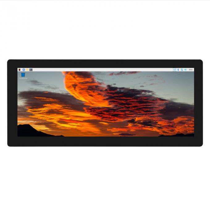
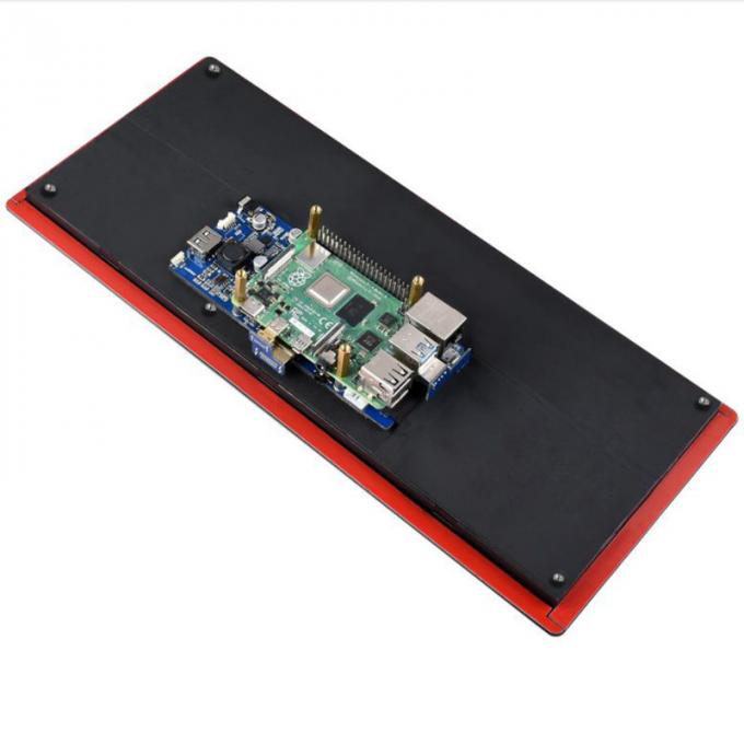
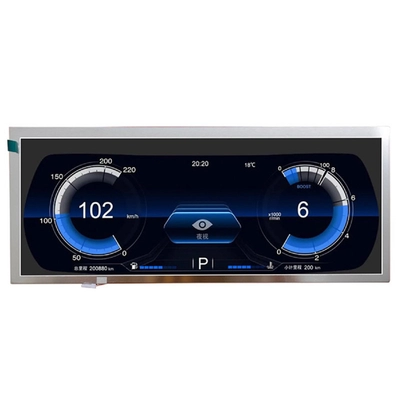
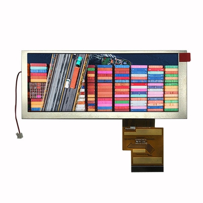
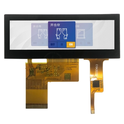
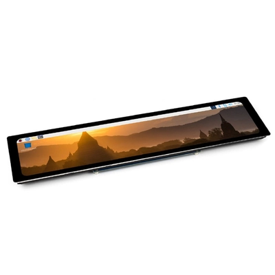
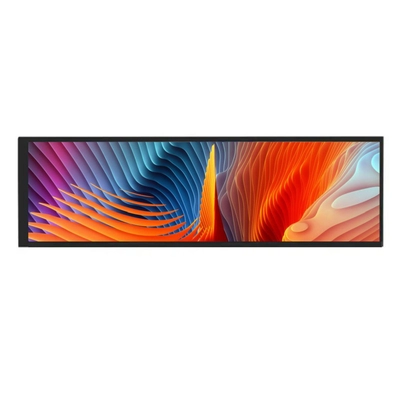
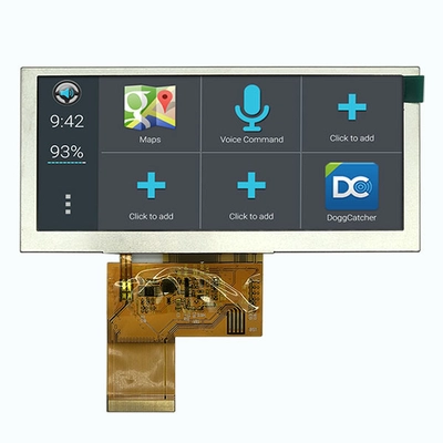
12.3 inch LVDS TFT High Brightness Display with PCAP Product Image
(without Capacitive Touch)

(with Capacitive Touch)


Reviews
There are no reviews yet.