Description
Unveiling the 3.5 Inch HVGA 320X480 MCU RGB TFT TN LCD Module ST7796S: A Next-Level Smart Device Display
Introducing the SHENZHEN TECHSTAR ELECTRONICS INCORPORATED CO., LTD SF-TC350H-8417A-N, a cutting-edge 3.5″ TFT-LCD display module boasting HVGA 320×480 resolution. Designed for seamless integration, this touch-sensitive LCD display module is effortlessly controlled by a variety of MCUs including 8051, PIC, AVR, ARDUINO, and ARM. Its versatility makes it ideal for a plethora of applications including embedded systems, automation, GPS, medical equipment, industrial devices, and security systems, all of which demand superior TFT display quality and vibrant imagery.
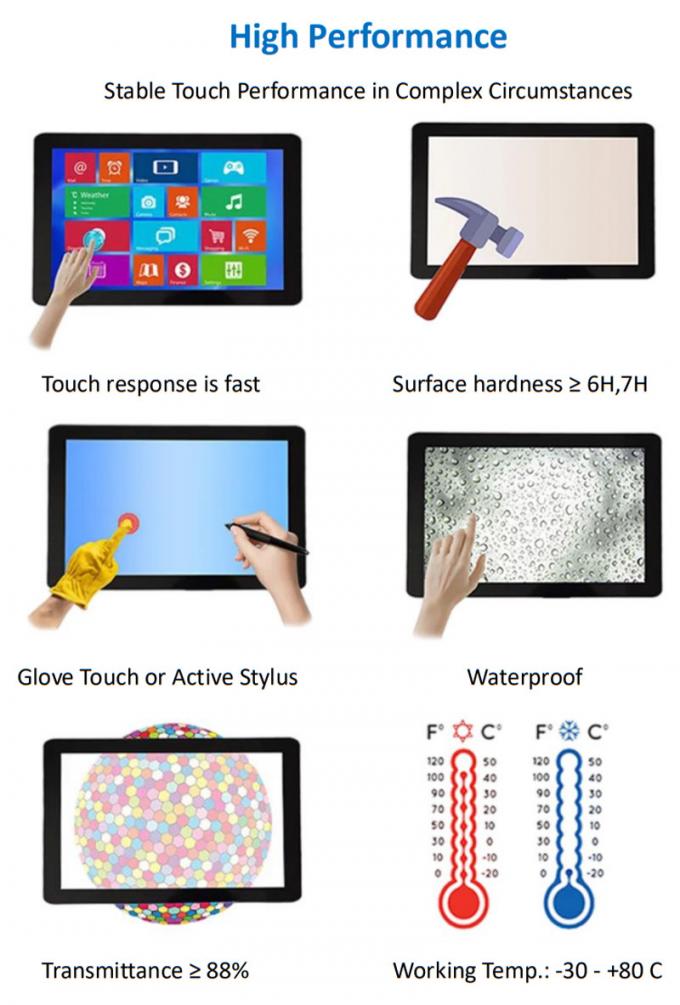
Operating within a temperature range of -20℃ to +70℃, with storage capabilities spanning from -30℃ to +80℃, the SF-TC350H-8417A-N module is engineered to endure diverse environmental conditions without compromising performance.
With a standard surface brightness of 200 cd/m2, tailored solutions are available for applications necessitating intensified backlighting, with customizable brightness options up to 1000 cd/m2. For further inquiries, please reach out to our dedicated sales team.
| Product: | 3.5 Inch TFT Display |
|---|---|
| Resolution: | 320×480 Pixels |
| Pin Number: | 45 Pins (Customizable) |
| Interface: | MCU +RGB Interface (Customizable) |
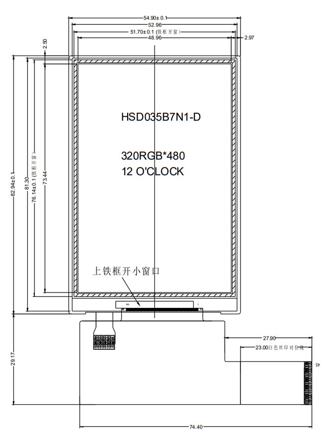
| Outline Dim.: | 54.9×82.94×2.1 Mm |
| Viewing Direction: | 12 O’clock |
| Touch Screen: | Without Touch Screen (Optional) |
| Driver IC: | ST7796S |
| Connection: | ZIF FPC (Can Be Customized) |
| Surface Luminance: | 200 Cd/m2 (Customizable) |
| Operating Temp.: | -20℃ To +70℃ |
| Compliance: | REACH & RoHS Compliant |
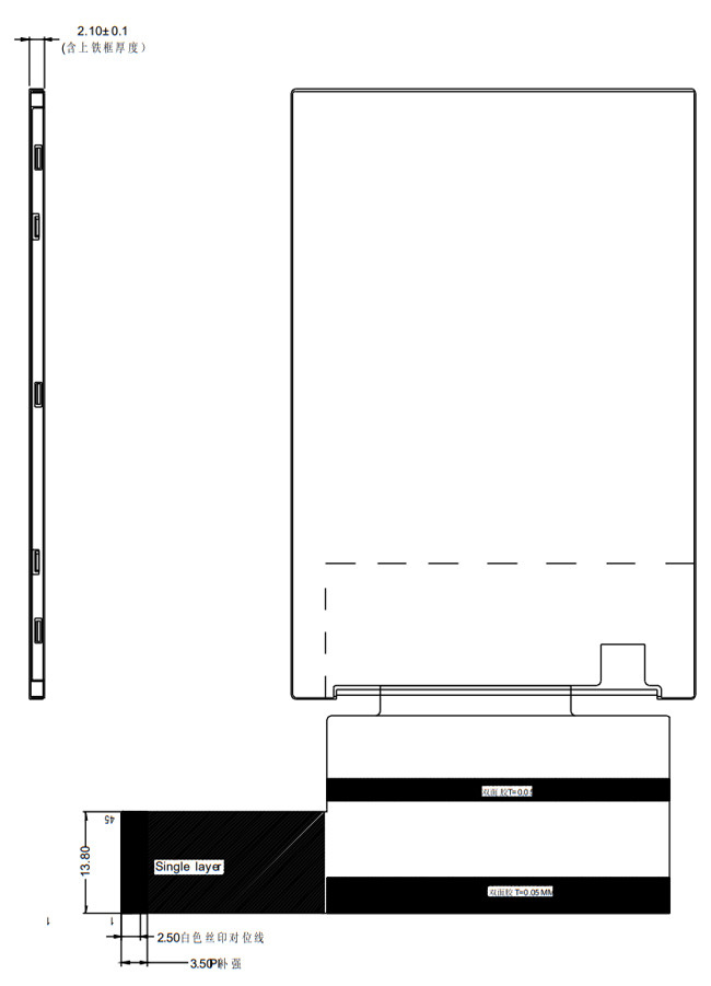
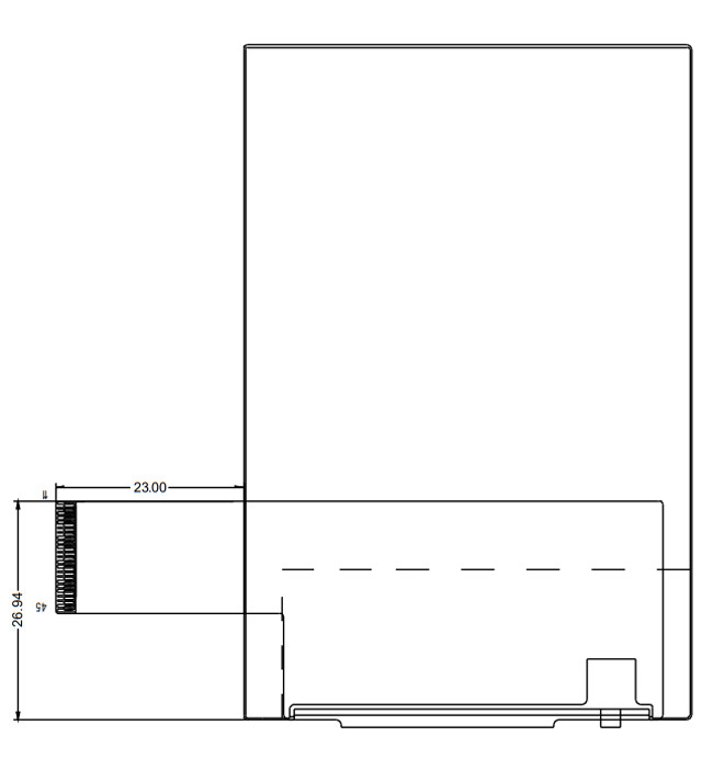
3.5 Inch 320X480 MCU& RGB TFT TN LCD Module Product Drawing
Interface Pin Definition
| NO. | PIN NAME | I/O | Description |
| 1-6 | K1-K6 | O | LED Cathode |
| 7 | A | O | LED Anode |
| 8 | GND | I | Ground |
| 9-10 | VCC | I | Power Supply 2.8V Voltage |
| 11 | NC | – | Set open |
| 12 | CS | I | Input pin for chip selection signal |
| 13 | RS | I | Register select signal |
| 14 | WR | I | Write strobe signal input pin |
| 15 | RD | I | Read strobe signal input pin |
| 16 | SDA | I | SPI Interface Input Pin |
| 17 | SDO | I | SPI Interface output Pin |
| 18-35 | DB0-DB17 | I/O | Display Data I/O |
| 36 | DE | I | Input Data enable control |
| 37 | DCLK | I | Clock Signal to Sample each date |
| 38 | HSYNC | I | Horizontal Synchronizing Signal |
| 39 | GND | I | Ground |
| 40 | VSYNC | I | Vertical Synchronizing Signal |
| 41 | RESET | I | LCM Reset input signal |
| 42-44 | IM2-IM0 | I | The MCU interface mode select. |
| 45 | GND | I | Ground |
DC Characteristics (VDD=2.8V,Ta=25°C)
| Item | Symbol | Min | Type | Max | Unit | Test condition |
| Operating voltage | VDD | 2.6 | 2.8 | 3.3 | V | – |
| Supply current | IDD | – | – | 5 | mA | VDD=2.8V,Ta=25°C |
| Input voltage | VIH | 0.8VDD | – | VDD | V | – |
| VIL | 0 | – | 0.2VDD | V | ||
| Input leakage current | IIL | -1.0 | – | 1.0 | mA | VIN=VDD or VSS |
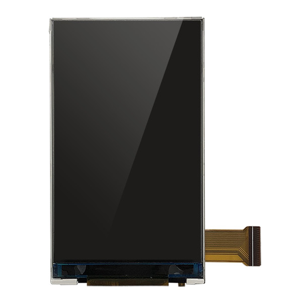
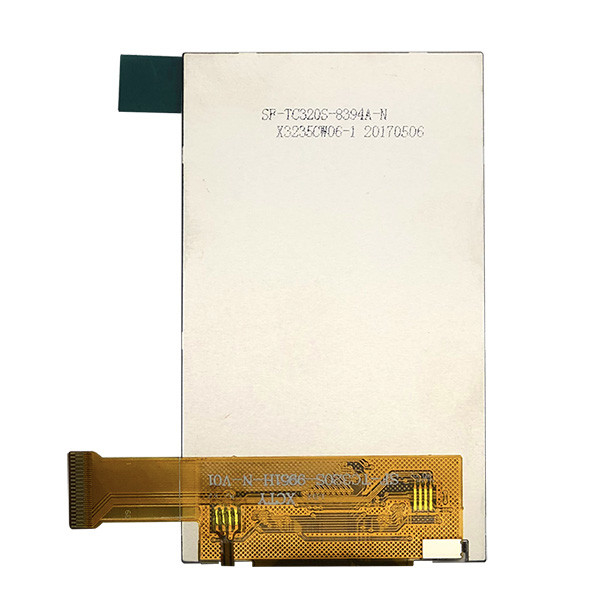
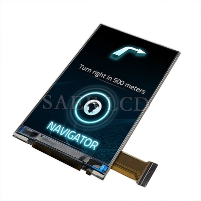
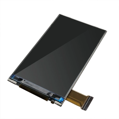
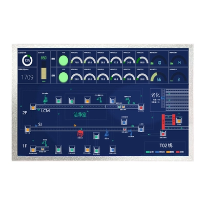
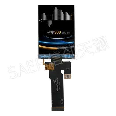
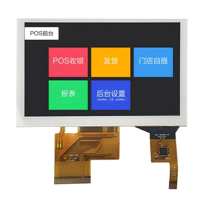
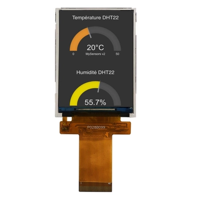
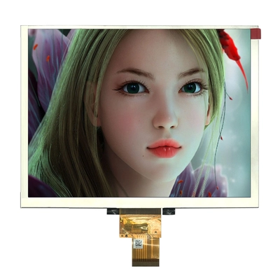
3.5 Inch 320X480 MCU& RGB TFT TN LCD Module Product Image


Reviews
There are no reviews yet.